INTRODUCTION.
For many years I have been modifying all manner
of Ku Uplink hardware down to 10 GHz.
The reason - the $cost of 10 GHz GaAs Power FET's is usually
prohibitive.
However, the problem with trying to modify the vast majority of Ku Band PA's down to 10 GHz lies with the GaAs FET Output Devices that Satellite Companies often use.
Ku Uplink hardware
operates in the range 14.00 through to 14.50 GHz. The
Manufacturers of Ku ODU usually design their Ku Band PA's with
“power” GaAs FET's that have a nominal specified Operating
Frequency Range of circa 13.5 GHz to 14.5 GHz.
The majority of these GaAs FET devices are IMFET's (Internally
Matched FET's). These IMFET devices have been deliberately
fabricated to (only) operate over a "limited" Frequency range.
This has been achieved by the inclusion of Inductive and
Capacitive elements within the FET structure.
Semiconductor manufacturers deliberately include these
"Reactive" elements to provide "stable" Gain across the
nominal Pass Band and NOT beyond.
The result is that these additional Reactive components have a
minimal effect within the Pass Band of the device but these
same components cause the device Gain to degrade outside of
this nominal Pass Band.
Our 10 GHz Amateur Band is clearly a long way outside (almost
3 GHz below) the Design Specifications of these Ku Band IMFET
devices. However, myself and indeed many other Amateurs have
found that many of these Ku Band IMFET's will deliver useful
performance (Gain) on 10 GHz.
The same scenario also applies to C Band IMFET's covering 5.9
-6.4 GHz and their reuse on 5.76 GHz.
However, there is one caveat on this Modification process!
The "retuning"
process around these IMFET's is often VERY tedious...
requiring many hours of fiddly "Snow Flaking".
On a more positive note – I recently, I acquired a quantity of
scrap 4 Watt Ku Band ODU's.
Once again I had to consider the value of the Ku Band Output
devices and their potential for 10 GHz Operations.
And so there was that usual lingering concern about the
significant effort required for "retuning" these Ku Band PA’s
versus the desired performance on 10 GHz.
To my great surprise, when I dismantled an ODU, I found the
ODU Manufacturer had used a pair of high Gain, Phased Ku
MMIC's from Eudyna. The Part Numbers used were FMM5081 and
FMM5059. Interestingly, both these MMIC’s differ physically
but the Eudyna Spec's for both look to be identical. They have
a specified Frequency range of 13.75 GHz to 14.5 GHz, a Gain
of circa 30 dB and they deliver more than 2 Watts.
With such a High Gain compared to that of a high power GaAs
FET (6-7 dB), if this Ku Band MMIC could be made to work on 10
GHz it would be a good cheap alternative to that ever popular
Eudyna X Band MMIC - FMM5061.
Amateur Radio Operators love the FMM5061 MMIC because of its
simplicity.
It delivers MORE than 2 Watts on 10368 MHz with circa 10 Milliwatts of RF drive. Although this MMIC is a very simple solution - delivering high Gain and good RF Power on 10 GHz, it has a couple of drawbacks.
The unit price is fairly costly at circa $US100
from multiple ePray Dealers and then one still needs to
find/fabricate a purpose built PCB to mount it etc.
NB : Down East Microwave (DEM) used to offer
this FMM5061 MMIC as a complete 3 Watt Amplifier Kit for more
than $US300 but it seems to have gone from their Sales
Inventory.
TECHNICAL
DISCUSSION.
With these thoughts in mind, I immediately set about the task
of modifying these Ku Band MMIC PA’s down to 10 GHz.
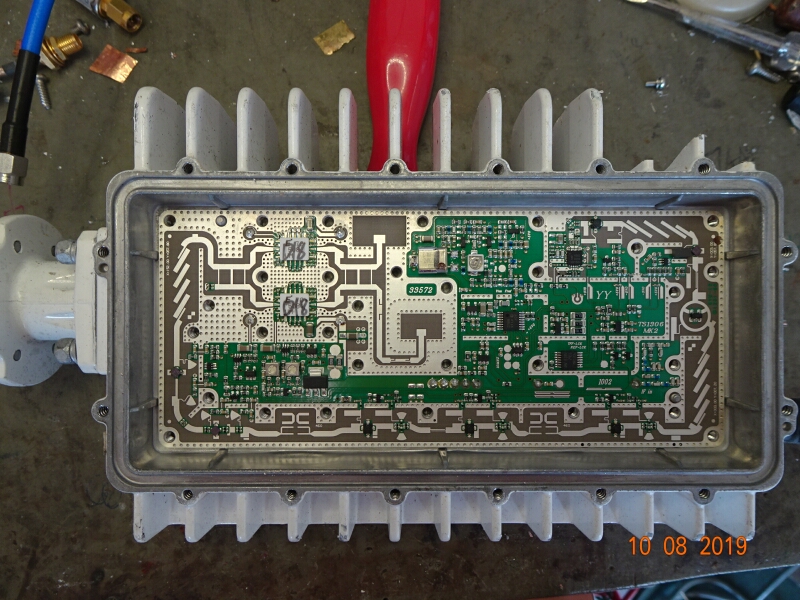
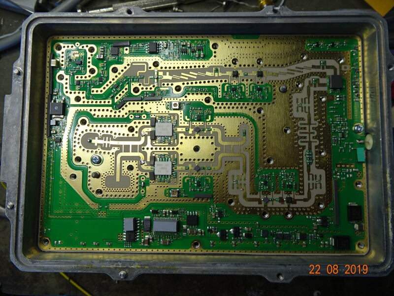
Here is a Photo of the Ku Band ODU main board.
The 2 off Phased
Eudyna MMIC's are top left.
There are 4 off PCB Pads for DC Supply Rails. The two on the
left are the -Vgg Bias Rails whilst the 2 on the right are the
+VDD Rails.
Note also the 2 off Wilkinson Splitters for the I/O Combining.
The Input Splitter has a discrete SMD 50 Ohm Balance Load
(lower left) while the Output Splitter has a coaxial "Pad"
above an integrated waveguide chamber as it's Balance Load
(upper right).
The 14 GHz RF output is coupled via it's longer Stripline
(lower right) to a coaxial "Pad" above another waveguide
chamber which ultimately couples towards the Feed Horn (Left).
And finally there are 2 Tuning "stubs" on the Output
Striplines immediately to the left of the Output Splitter.
All of these frequency dependent "elements" have been designed
for Ku Band functionality.
So... if we wish
to use this MMIC in a potential 10 GHz application these
"elements" must be removed (Scalpel) leaving only the I/O
Striplines that feed the individual MMIC's.
MODIFICATION
PROCESS.
This description has been written on the basis that any
Operator can emulate the actions I have implemented on similar
alternate Ku Band ODU’s.
Most Ku Band ODU’s
operate from a single circa +20 Volt Supply. Since both MMIC's
were already mounted on a PCB with Heatsinking and complete
with their DC supply rails, I decided to attempt a
Modification within the original case/hardware.
With the knowledge that all GaAs FET's need some form of DC
isolation in their RF ports, I initially fitted SMD DC
Isolation capacitors (3.9pf) in each Stripline. However,
this was later found to be unnecessary because the Eudyna
Datasheet shows "integrated" DC isolation was already
included.
So... the next
task was to fit I/O Coax tails to couple the RF In/Out of each
MMIC. To achieve the best possible RF coupling, each I/O
Coax needs a good Ground Plane. To achieve this I decided to
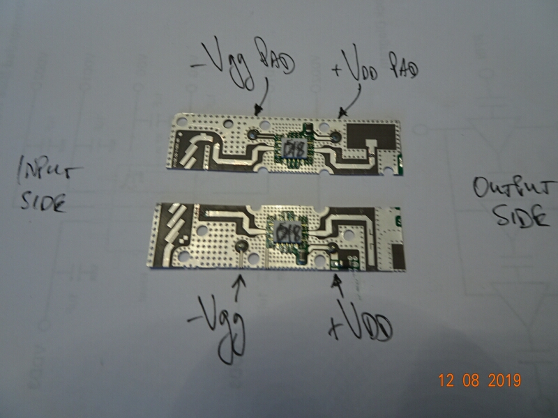
solder some copper "shim" material linking as much of the
existing Ground Planes as possible. While there are slight
layout differences between each MMIC PCB (refer Photo below),
the RF Earthing issues will be fairly obvious to see/work out.
For the Coax connections, I initially tried .141 Hardline but
the large physical step from the PCB Track to the centre
conductor caused RF Coupling issues. The smaller .085 Hardline
is a much better choice but I finally settled on using some
flexible Teflon tails that I had scavenged from other
equipment.
I then soldered in these short Coax Tails to the I/O Strip
Lines and the newly created Ground Planes.
A Power Meter (HP435A) was connected via a 30 dB Attenuator.
After Powering Up the ODU, I checked the +VDD and -Vgg Supply
rails and then Set the RF Drive to +13 dBm.
I immediately saw a few 100 Milliwatts of RF Output. This was
a very positive result for an as yet "untuned" PA.
Over the next few hours I ultimately found the simplest "Snow
Flaking" solution that delivered the highest Gain
with maximum Output.
The final result was more than +30 dBm Output (1.2 Watts
typical) with +13 dBm Drive.
A Drive level of +10 dBm delivers circa 750 Milliwatts.
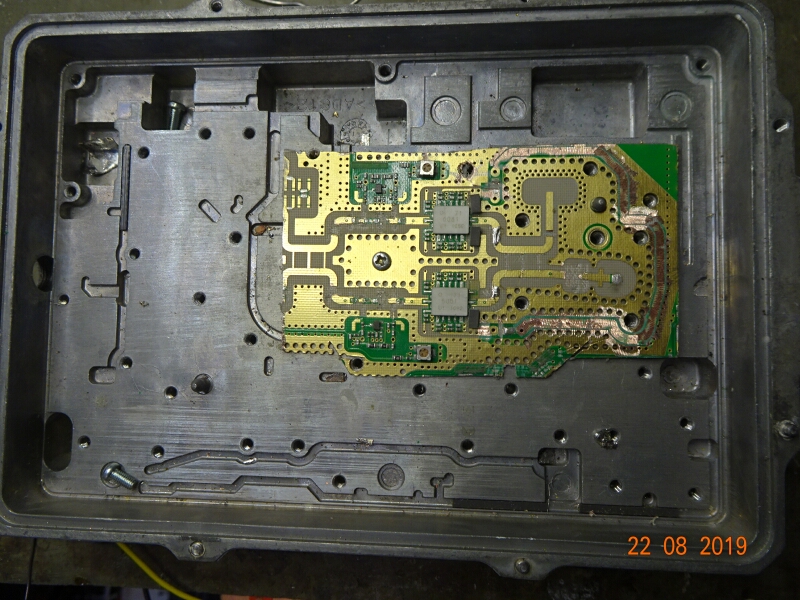
With such a pleasing result I then decided to remove (cut)
these dual MMIC PA's from the Main PCB and to split
them into separate amplifiers. These PCB’s are VERY small !!
They are only 70mm X 18mm.
In USA parlance... that’s less than 3 Inches long and only ¾ Inch wide.
Once again, all Frequency dependent "elements"
were removed leaving just the I/O Striplines feeding the
MMIC's.
When I first mounted the top PCB to a Heatsink I discovered I had DC short circuit problems. It turned out that I had missed seeing that each PCB has Through Hole Plated DC Pads for both +VDD and the -Vgg Supply Rails. My alternate Heatsink effectively shorted these exposed Pads to Earth. To overcome this, I had to either drill a small countersunk hole in the Heatsink directly under this Pad or simply suck the solder out of this Pad and use a small Drill to eliminate the contact point of Through Hole "Pad" on the underside of the PCB before Mounting on the Heatsink. For the lower PCB, I also had to solder a very fine wire from the Vgg Bias connection to it’s Bias Pad marked –Vgg.
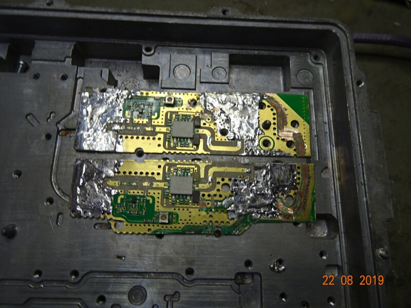
The next part of the process was the creation of the Ground Planes for each of the I/O Coax tails.
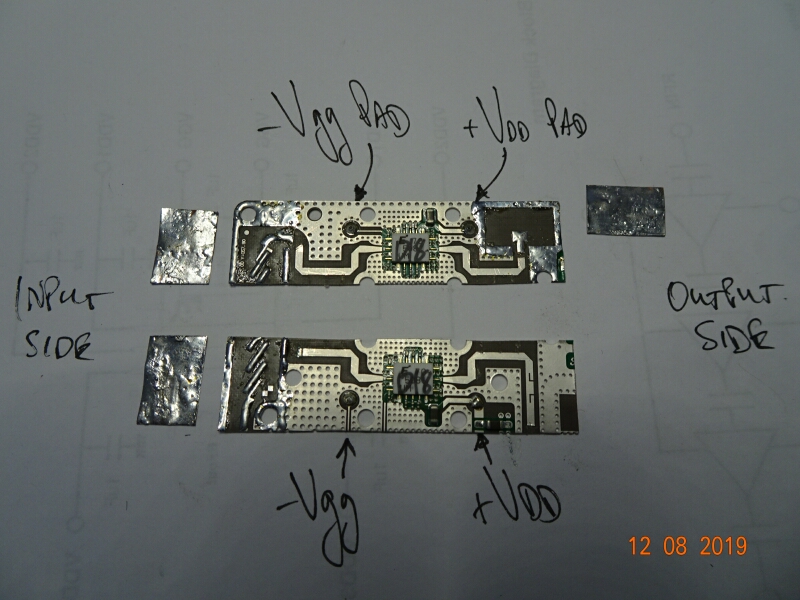
To maximise adhesion of the “tinned” copper
shim material, on the Input I chose to leave all the RF Tracks
intact.
So... I "tinned" all surrounding copper tracks on the PCB and
then lapped the preformed shim over the entire surface and
soldered it.
Note also the I/O Striplines have been trimmed ready for their
RF connections.
Below is a Photo of the completed Ground
Planes.
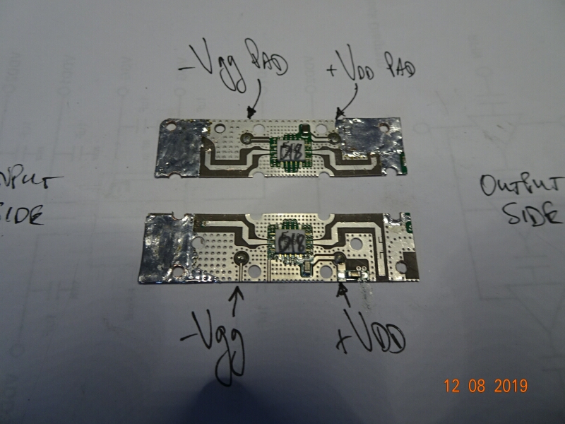
Readers will hopefully note that I have restored (created) the PCB Mounting holes. I suggest 8 holes are needed for best RF Grounding. I cannot emphasise enough how important it is to fit all 8 Screws (3mm ? or Self Tappers) to ensure best RF Grounding. Poor RF Grounding means reduced Output !!!
A mandatory smear of Heat Sink Compound under the MMIC is also
necessary to achieve optimum heat transfer.
After carefully mounting the PCB on a suitable Heatsink, I
then fitted the I/O Coax tails and repeated the "Snow Flake"
(retune) task. For the most part, there are only 3 or 4
Snowflakes needed to optimise this PA.
The final result
can be seen here in this Photo
of a single Amplifier.
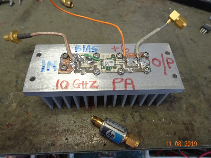
This Amplifier requires 2 Supply Rails... a Negative Bias Rail Vgg (Green wire) of circa -0.20 Volts and +VDD Rail in the range +5 to +6 Volts maximum.
The +VDD Rail is simply a short piece of hookup wire (Orange
wire) on the O/P side of the MMIC.
A similar arrangement can be adopted for the Vgg Supply.
Missing is a mandatory Earth wire.
Note that for this PA the -Vgg Bias Rail (now) appears on an
SMD capacitor that I soldered directly to the PCB.
To achieve the quite low -Vgg Voltage Rail of circa -0.20
Volts, I used a -5 Volt Supply developed from a 7660 Chip or
similar. This -5 Volts is coupled to a 3.9K Resistor in series
with a 1K Pot.
The centre of this Pot delivers a maximum of -1.0 Volts.
The reason for this Bias arrangement is because the Absolute Maximum Bias voltage for this MMIC is -3.0 Volts.
Before I connected the +6 Volt VDD Rail, I preset the -Vgg Rail to circa -1.0 Volts to “Set” the PA at Cut Off.
This ensures the
MMIC will not destroy itself if the +6 Volt VDD Supply rail is
NOT Current Limited (i.e. 2 Amps max).
The recommended quiescent IDD for these MMIC's is 1200 mA.
To achieve this IDD, I carefully reduced the -Vgg voltage whilst monitoring the +6 Volt IDD current.
The final -Vgg Bias voltage for this MMIC was circa -0.20 Volts.
The application of RF Drive will push this IDD current up towards 1.5 Amps and more, hence the need for an adequate Heatsink or small Fan.
MODIFYING
ALTERNATE Ku BAND ODU's.
As I stated earlier, this Modification process is easily
adaptable to similar RF hardware.
The PCB design is different but the MMIC’s are the same and as a result similar RF performance was achieved on 10 GHz.
Once again there are a pair of phased Ku Band MMIC’s in the above ODU.
This Photo shows only the
Ku RF Amplifier chain.
The MMIC’s have been excised from the main PCB. All
unnecessary Tracks, components, and tuning Stubs must be
removed in preparation for Snow Flaking and the creation of
the I/O Ground Planes.
This Photo shows the
modified and now separated MMIC PCB’s with the somewhat
untidy Ground Planes in place.
The next part of the
process is identical to that previously described.
So... fit the I/O Coax’s, the DC connections for the VGG
& VDD rails and then Snow Flake the I/O strip-lines for
optimum performance etc.
This Project and my Modification description is now more than
3 years old.
Unfortunately, all the Free MMIC PA's I offered have run out.
Many have gone to International Operators - which for me is
very pleasing.
I surely hope they find their way to On Air stations.
To find similar
hardware... I suggest AR Ops keep a look out for surplus Ku
Band ODU's at Flea Markets etc.
Good Luck !
Cheers,
Alan - VK3XPD